
Avoid Thermal Stress in Prototype Circuit Board Assembly
Prototype circuit board assembly is a vital step in the electronic design process. It transforms schematics into a physical printed circuit board (PCB) for testing and evaluation before the product goes to manufacturing. However, if the PCB is exposed to thermal shock during prototyping, it may not work as intended. Thermal stress can cause the PCB to delaminate or to fail in other ways, depending on the conditions involved. This article will explore how thermal stress affects the prototype circuit board assembly process and what steps original equipment manufacturers (OEMs) and electronics manufacturing services providers (EMS providers) can take to avoid it.
Thermal shock refers to the effects of extreme temperatures on a printed circuit board (PCB). The temperature variations can cause damage through a variety of mechanisms, including metal fatigue, corrosion, embrittlement, or even fracture and disconnection. These effects are exacerbated when the circuit board is subjected to repeated cycles of high and low temperatures. The resulting stresses can cause the copper layers of the PCB to separate from the dielectric material, affecting signal paths or even causing failure altogether.
When a circuit board is assembled, it undergoes mechanical and electrical testing to ensure it can be reliably put into service. Mechanical tests include visual and X-ray inspection, peel testing, and solder pot and float tests. Electrical testing includes in-circuit and environmental stress screening as well as functional testing. While these tests help ensure the final prototype is up to spec, they can also add time to the overall assembly process. As a result, OEMs and EMS providers should select assemblers with quick-turnaround manual assembly capabilities to accommodate revisions quickly and reduce the impact of time-consuming retests on their prototype circuit board assembly process.
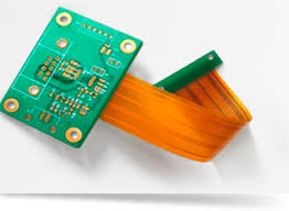
How Do You Avoid Thermal Stress in Prototype Circuit Board Assembly?
The risks of thermal shock can be avoided through proper PCB layout and materials selection, along with thorough testing. Designers can minimize thermal stress by selecting PCB substrate and component materials with matching CTE values, and by properly positioning components to disperse heat across the entire surface area of the board. They can also consider adding thermal vias or incorporating thermal patterns in their designs to dissipate heat more efficiently.
As the electronics industry evolves, new technologies are reshaping prototype pcb assembly processes. Advanced software is allowing engineers to run simulations of their designs and predict any potential issues before production begins. This prevents costly errors and enables a faster path to market.
Whether you’re an OEM, a startup, or an engineer, you must understand the intricacies of prototype PCB assembly to produce high-quality products that meet customer demands. By ensuring that the assembly and test processes are tightly controlled, you can avoid the dangers of thermal shock and speed up your path to a successful launch. RayMing’s experts can guide you through the nuances of prototyping and production, from initial concept to final assembly. Contact us today for more information.